- 您现在的位置:买卖IC网 > Sheet目录1994 > DS3106LN+ (Maxim Integrated Products)IC TIMING LINE CARD 64-LQFP
DS3106
33
Table 7-17. OC3 Default Frequency Configuration
O3F[2:0]
SONSDH
FREQUENCY
(MHz)
O6F[2:0]
=001
OFREQ3
APLL
SRC
000
X
0
X
0000
—
001
0
8.192
FALSE
1101
T4
1
6.176
1101
T4
001
0
8.192
TRUE
0111
T0
1
12.352
0111
T0
010
0
68.736
X
1111
T4
010
1
22.368
X
1110
T4
011*
X
19.44
X
0110
T0
100
X
25.92
X
0111
T0
101
X
38.88
X
1000
T0
110
X
51.84
X
1001
T0
111
X
77.76
X
1010
T0
*Occurs when O3F[2:0] are left unconnected.
7.8.2.5 FSYNC and MFSYNC Configuration
The FSYNC output is enabled by setting FSEN = 1 in the OCR4 register, while the MFSYNC output is enabled by
setting MFSEN = 1 in OCR4. When disabled, these pins are driven low.
When 8KPUL = 0 in FSCR1, FSYNC is configured as an 8kHz clock with 50% duty cycle. When 8KPUL = 1,
FSYNC is an 8kHz frame sync that pulses low once every 125
s with pulse width equal to one cycle of output
clock OC3. When 8KINV = 1 in FSCR1, the clock or pulse polarity of FSYNC is inverted.
When 2KPUL = 0 in FSCR1, MFSYNC is configured as an 2kHz clock with 50% duty cycle. When 2KPUL = 1,
MFSYNC is a 2kHz frame sync that pulses low once every 500
s with pulse width equal to one cycle of output
clock OC3. When 2KINV = 1 in FSCR1, the clock or pulse polarity f MFSYNC is inverted.
If either 8KPUL = 1 or 2KPUL = 1, output clock OC3 must be generated from the T0 DPLL and must be configured
for a frequency of 1.544MHz or higher or the FSYNC/MFSYNC pulses may not be generated correctly. Figure 7-3
shows how the 8KPUL and 8KINV control bits affect the FSYNC output. The 2KPUL and 2KINV bits have an
identical effect on MFSYNC.
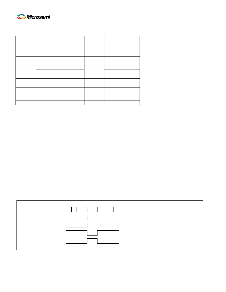
Figure 7-3. FSYNC 8kHz Options
OC3 OUTPUT CLOCK
FSYNC, 8KPUL=0, 8KINV=0
FSYNC, 8KPUL=0, 8KINV=1
FSYNC, 8KPUL=1, 8KINV=0
FSYNC, 8KPUL=1, 8KINV=1
发布紧急采购,3分钟左右您将得到回复。
相关PDF资料
DS3231MZ+
IC RTC I2C 8SOIC
DS3231SN#T&R
IC RTC W/TCXO 16-SOIC
DS3232MZ+
IC RTC W/SRAM I2C 8SOIC
DS3232SN#T&R
IC RTC W/TCXO 20-SOIC
DS3234S#
IC RTC W/TCXO 20-SOIC
DS32C35-33#T&R
IC RTC ACCURATE I2C 3.3V 20-SOIC
DS3911T+
IC DAC 10BIT I2C QUAD 14TDFN
DS4000KI/WBGA
IC OSC TCXO 19.44MHZ 24-BGA
相关代理商/技术参数
DS3107FP000
制造商:Thomas & Betts 功能描述:30A,CON,2P3W,MG,107,125V
DS3107FRAB0
制造商:Thomas & Betts 功能描述:30A,REC,2P3W,MG,107,AB0,125,SC
DS3107MP000
制造商:Thomas & Betts 功能描述:30A,PLG,2P3W,MG,107,125V
DS3107MP00K
制造商:Thomas & Betts 功能描述:30A,PLG,2P3W,MG,107,125V,CC
DS3107MR000
制造商:Thomas & Betts 功能描述:30A,NLT,2P3W,MG,107,125V
DS3107MRAB0
制造商:Thomas & Betts 功能描述:30A,NLT,2P3W,MG,107,AB0,125V
DS3108A14S5S621
制造商:Amphenol Corporation 功能描述:
DS3108A14S6S
制造商:Amphenol Corporation 功能描述: